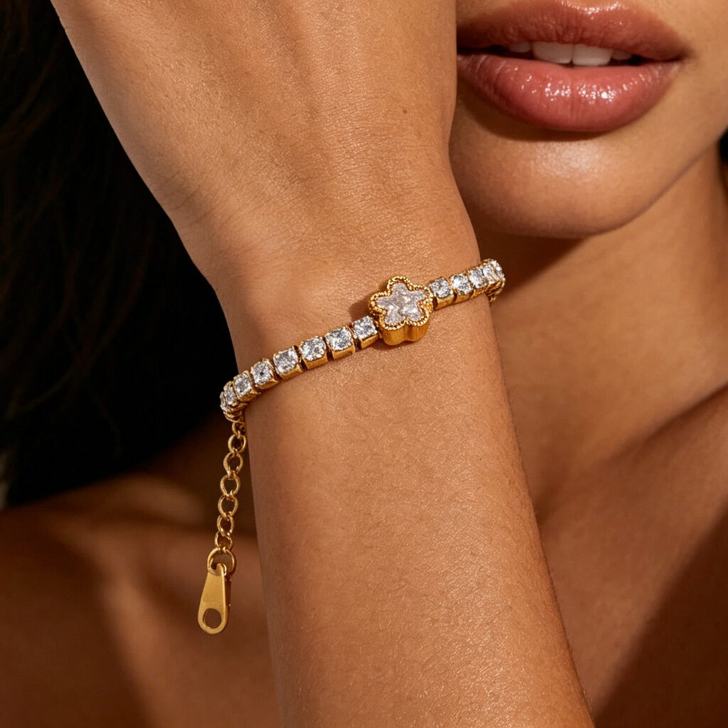
PVD Coating Thickness Explained directly impacts product longevity and profit margins. Incorrect specifications lead to premature wear, costly warranty claims, and blurred fine details for jewelry.
This analysis benchmarks optimal PVD coating ranges against industry standards. We evaluate specific thickness requirements, aus 0.03-0.08 µm for fashion jewelry to 2.0-5.0 µm for functional applications, to help you define exact specifications.
What Is PVD Coating Thickness?
PVD coating thickness defines the thin film’s physical depth, applied for specific functional or decorative properties. It is critical for part performance and precision.
Definition and Typical Ranges of PVD Coating Thickness
PVD coating thickness refers to the physical depth of the thin film layer. This typically ranges from sub-micron to several microns. Manufacturers apply this layer via Physical Vapor Deposition to achieve specific functional or decorative properties.
General industrial PVD coatings commonly range from submicron (less than 1 µm) to several microns. Many precision applications stay below 5 µm.
Decorative PVD coatings are approximately 0.30–1.0 µm thick. They serve primarily for aesthetic finish and light scratch resistance.
Functional PVD coatings, such as those for wear resistance or tooling, are typically 2.0–5.0 µm thick.
Aerospace standard AMS 2444A defines TiN PVD coating thickness classes: Class 1 (1.27–3.81 µm), Class 2 (2.54–6.10 µm), and Class 3 (6.35–12.70 µm).
Compared to other methods, PVD coatings are generally thinner (less than 5 µm) and ideal for precision. Chemical Vapor Deposition (CVD) coatings are much thicker, at 25–75 µm.
Significance and Application of PVD Coating Thickness
Functional Performance: Thickness directly impacts wear resistance, increasing it by 200–400% over uncoated parts. It improves barrier properties for corrosion resistance and maintains surface hardness, usually around 2000–3500 HV.
Mechanical Behavior: PVD coating thickness affects how the material deforms and cracks. Thinner films may exhibit columnar cracking, while thicker films can show inclined or edge cracking due to internal stress.
Dimensional Precision: Thin PVD coatings, often less than 5 µm, are suitable for precision components. Things like cutting tools benefit because these coatings maintain tight tolerances and original part geometry.
Optimization: Selecting the right thickness involves balancing the need for wear and corrosion protection with managing internal residual stress. Too much stress can lead to cracking or delamination in thicker films.
Substrate Influence: Harder substrates better support thinner, higher-stress coatings. Softer substrates need careful thickness consideration to manage stress and prevent premature failure.
Measurement: Techniques like X-ray Fluorescence (RFA) and instrumented nanoindentation accurately measure PVD coating thickness. This verifies compliance with specifications.
Design Guidelines: Effective design considers the primary function (aesthetic, moderate, or high wear). This matches thickness to substrate hardness, contact conditions, and dimensional requirements. Performance testing follows.
How Is PVD Coating Thickness Measured?
We measure PVD coating thickness both during the process and after, using precise tools for quality checks and process control.
Measuring PVD coating thickness requires high-resolution methods. Coatings typically range from sub-micron up to about 10–15 µm. We use a mix of real-time monitoring during deposition and post-process checks on finished parts.
In-Process PVD Thickness Monitoring
In-process methods track or control thickness while we’re depositing the coating. This helps hit our target micrometer range and maintain uniformity.
- Quartz Crystal Microbalance (QCM): A QCM sensor sits inside the PVD chamber. Mass buildup on the crystal changes its resonant frequency. We calibrate the deposition rate, then the system estimates film thickness against time. This works well for metallic and nitride coatings in the 1–10 µm range, especially for production batches.
- Optical Monitoring (Ellipsometry, Optical Emission, Spectroscopy): Optical emission spectroscopy follows plasma emission lines, telling us about deposition conditions. Ellipsometry measures changes in reflected light’s polarization, giving film thickness and refractive index. We use these methods for precise thickness control on thin, optical, or semi-transparent layers. They are non-contact, so they fit well into automated high-volume lines.
- Real-Time Monitoring Devices and Feedback Control: We integrate real-time sensors like optical units, QCMs, and process probes. These feed data into control software. Our algorithms adjust for substrate variations and process drift, keeping thickness consistent across batches. Zum Beispiel, we create a deposition rate curve for each coating type and substrate, then use in-situ monitoring to stop deposition when the target thickness is met.
Post-Process PVD Thickness Measurement
After coating, we use various methods to measure the finished part. This is for quality assurance, process validation, and certification.
- X-Ray Fluorescence (RFA): XRF is a non-destructive method we widely use for PVD thickness on metallic and alloy substrates. An X-ray beam excites the coating, and we analyze the emitted X-rays to get both composition and thickness. Modern units can measure up to five layers at once, which is great for multi-layer PVD stacks. This method often verifies compliance with standards like AMS 2444A.
- Magnetic Induction (for Ferromagnetic Substrates): We use this method when a non-magnetic PVD coating goes onto a ferromagnetic substrate like steel. A probe generates a magnetic field. The field strength changes with the coating thickness. The instrument converts this signal into a thickness reading using a calibrated function. It works best for coatings over 1 µm.
- Eddy Current (for Non-Ferrous Substrates): This applies to non-magnetic, electrically conductive substrates such as aluminum or copper. A high-frequency current creates eddy currents in the substrate. Changes in the response, like amplitude or phase shift, tell us the coating thickness. It’s good for metallic PVD layers on non-ferrous metals.
- Ultrasound-Based Methods: Ultrasonic gauges send sound waves through the coating and pick up reflections from layer interfaces. Time-of-flight data, with known sound velocity, gives us thickness. We mainly use this for coatings over 1 µm, where the acoustic impedance difference is clear enough.
- Beta-Backscatter (Radiation-Based): An isotope emits beta particles that go through both coating and substrate. We detect backscattered particles at 180 degrees. The thickness is calculated from the backscatter intensity. This needs at least a 5 atomic number difference between the coating and substrate. While historically used, XRF has largely replaced it in many applications.
- Instrumented Indentation / Nanoindentation: This involves recording a force-displacement curve as an indenter pushes into the coating. For coatings thicker than about 1 µm, we can estimate thickness from this curve, as the substrate’s influence becomes clear after about 10% penetration. It’s often used for hard PVD layers, like on cutting tools, also giving us hardness and modulus data.
- Cross-Sectional Microscopy (Destructive): We prepare a sample by cutting, mounting, and polishing it to expose a cross-section of the coated substrate. Then, we use an optical microscope or SEM to directly measure coating thickness from calibrated images. This is a destructive method, but it provides highly accurate reference data for calibrating non-destructive methods.
- Ball Crater (Calotte Grinding) Method: This involves grinding a spherical crater into the coated surface with a rotating ball and abrasive slurry. By measuring the crater diameters in the coating and substrate, we can geometrically calculate the coating thickness. It’s destructive but effective for quality control sampling and correlating with tool wear performance, especially on complex 3D geometries.
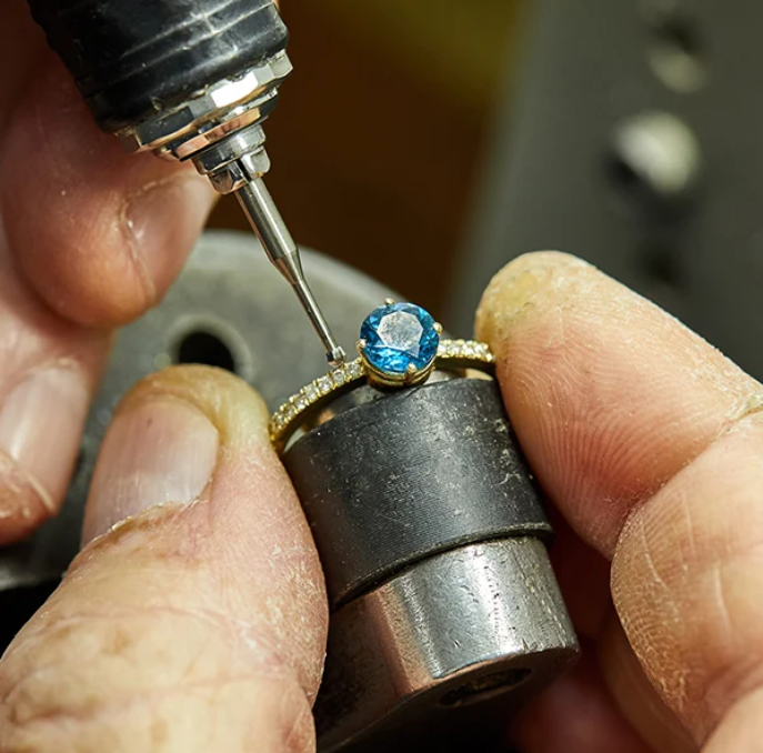
Unlock High Margins with Custom Jewelry Manufacturing
What Unit Is Used to Measure PVD Thickness?
PVD thickness relies on micrometers for functional layers, nanometers for ultra-thin films, and mil in North American imperial contexts. These units integrate across different industrial standards.
Key Measurement Units for PVD Thickness
- Micrometers (µm) are the dominant standard for functional and decorative PVD layers, often specified in ranges like 1 Zu 10 µm for hard coatings.
- Nanometers (nm) are preferred for ultra-thin, optical, or barrier PVD films, commonly specified in the range of 50–500 nm.
- Mil (0.001 inch) is used in North American industries for compatibility with imperial specifications, where 1 mil is approximately 25.4 µm.
Unit Usage in Specifications and Measurement Systems
- Industry standards and specifications primarily define PVD thickness in micrometers, while nanometers are common in high-precision and optical applications.
- Measurement tools such as X-ray fluorescence (RFA) and ultrasonic gauges typically output thickness in micrometers, with options for nanometers or mil depending on the system.
- Important conversion relationships include 1 µm = 1000 nm and 1 mil = 25.4 µm, which help integrate PVD thickness data across different regional or industrial standards.
Wie dick ist die PVD-Beschichtung auf Schmuck??
PVD-Beschichtungen auf Schmuck sind ultradünn, usually sub-micron, but provide high durability. This comes from balancing optimal thickness with material hardness and strong adhesion.
Common PVD Coating Thicknesses in Jewelry
PVD coatings on jewelry are thin layers, much thinner than a human hair, but still provide excellent protection and color. Most jewelry PVD is in the sub-micron to low-micron range.
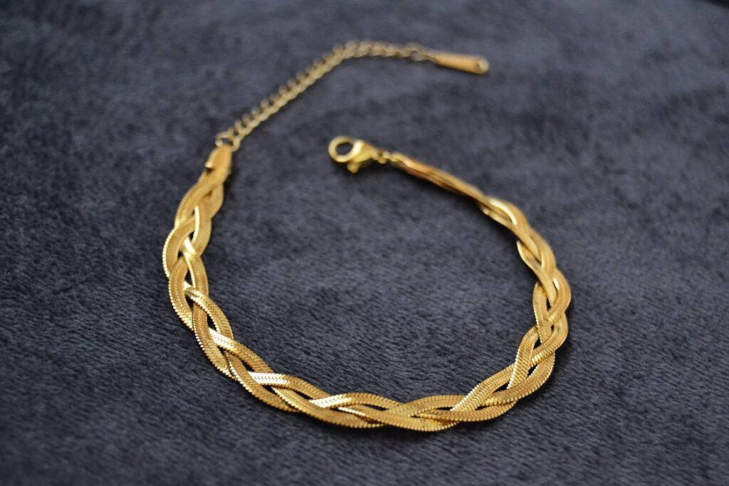
For mass-market stainless steel fashion jewelry, a thickness of **0.03–0.08 µm** is common. This range effectively preserves fine details like engravings and micro-textures. It also offers good adhesion, Härte, and ductility, balancing performance with cost.
Higher-quality decorative jewelry, including mid- to high-end stainless steel and some watch components, typically uses **0.1–1.0 µm**. Some manufacturers also consider **≥0.5 µm** a practical minimum for „good“ durability in daily wear. You might see broader ranges like **0.25–5 µm** for specialized jewelry or watch parts that need more wear resistance.
It is critical to understand that PVD coatings achieve their durability through hardness and molecular bonding, not just sheer thickness. A thin PVD layer often outperforms much thicker traditional gold plating.
Factors Influencing PVD Jewelry Durability and Service Life
Many elements affect how long PVD-coated jewelry lasts. Thickness plays a role, but it is not the only factor. Here is what matters:
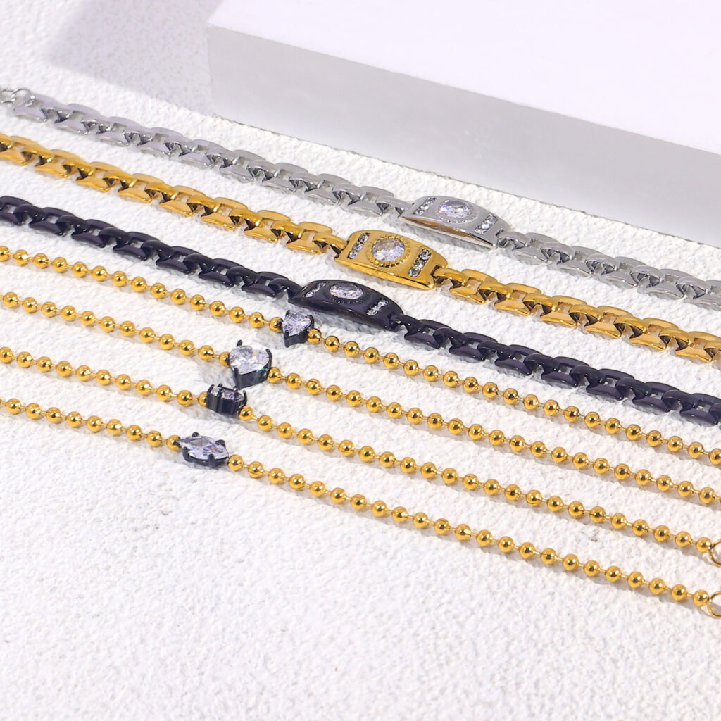
- Base Metal or Substrate: 316L stainless steel is the preferred base. It is corrosion-resistant and bonds well with PVD. A harder substrate supports thinner coatings better.
- Wear Area and Contact Type: Rings and bracelets endure more friction. These pieces benefit from thicker decorative PVD, often **≥0.1–0.5 µm**. Earrings and pendants, with less contact, do well with thinner coatings like **0.03–0.1 µm**.
- Desired Lifetime and Use Conditions: For everyday wear, **0.03–0.08 µm** on stainless steel often lasts about 2–3 years. For 3–5+ years, look for **0.1–0.5 µm** and good process control. Harsh conditions like chlorinated pools or heavy manual work will shorten life, no matter the thickness.
- Coating Material and Chemistry: Different PVD materials like TiN, ZrN, or DLC have unique hardness and stress levels. These properties influence how thick the coating can be without cracking.
- Production Economics: Thicker coatings mean more material and longer chamber time. Manufacturers balance cost with target lifetime. For many stainless steel fashion lines, the **0.03–0.08 µm** range is a cost-effective choice.
- Adhesion and Internal Stress: PVD bonds at a molecular level, giving excellent adhesion. Too much thickness, though, can increase internal stress. This causes cracking or delamination, reducing overall endurance. Thin-film ranges like **0.03–0.08 µm** are a good balance of adhesion, Härte, and ductility.
- Process Quality and Uniformity: The method and parameters of deposition, along with proper surface preparation, are crucial. A well-applied, uniform coating, even if thinner, often performs better than a thick, inconsistent one.
These factors combine to dictate how long PVD jewelry maintains its appearance and integrity. Good PVD coating quality comes from optimizing all these elements for the specific product and its intended use, not just piling on thickness.
Does Thicker PVD Coating Mean Better Quality?
Thicker PVD coating does not automatically mean better quality. Optimal thickness is application-specific, where excessive thickness can reduce performance or increase costs.
Key Factors Determining PVD Coating Quality Beyond Thickness
PVD coating performance relies on many interacting factors, not just thickness. To get a high-quality PVD coat, you need to consider more than just how much material is there.
- Coating Material Chemistry: The type of material, wie TiN, CrN, or DLC, determines intrinsic properties such as hardness, friction, und Korrosionsbeständigkeit.
- Thickness Uniformity: Consistent thickness across the part is crucial. An uneven coating can lead to weak spots or over-thick regions with high stress.
- Haftung: The bond between the coating and the substrate matters. A strong bond prevents peeling or delamination.
- Hardness and Toughness: The coating’s ability to resist deformation and fracturing is key for durability.
- Residual Stress and Microstructure: Internal stresses and the way the coating’s atoms arrange affect its stability and resistance to cracking.
- Substrate Material and Hardness: The underlying material must properly support the coating. A hard coating on a soft substrate might fail because the substrate deforms.
- Environment and Use Case: How the part is used—its exposure to corrosion, abrasion, impact, or high temperatures—significantly affects how well the coating performs.
- Prozesskontrolle: Precise control of deposition conditions ensures consistent quality from batch to batch.
High-quality coatings show no color differences, no delamination, and provide the right hardness and wear resistance for the job. Thickness is just one part of this equation.
Optimizing Thickness: When It Helps, Hurts, or Is Just Right
Finding the right PVD coating thickness is about balance. Too little, and it fails fast. Too much, and you run into new problems. The goal is the minimum thickness that meets performance goals without creating new issues.
Increasing thickness can bring benefits, but only up to a certain point:
- Improved Wear Life: More material means longer resistance to abrasion before the substrate shows. This increases tool or component life when adhesion and stress are controlled.
- Better Protection for Heavy Contact: For parts under significant load or gouging, thicker PVD with a hard substrate prevents premature breakthrough.
- Enhanced Corrosion Resistance: A denser, adequately thick coating with fewer defects improves barrier properties against corrosive attack.
- Meets Standards: Some aerospace and industrial specifications require minimum thickness classes to meet specific performance targets.
Jedoch, there are clear downsides to excessive thickness:
- Higher Internal Stress: PVD films have internal stresses. As they get thicker, this stored energy can lead to cracking, buckling, oder abblättern, making the coating unstable.
- Reduced Adhesion: Thick, high-stress films are more likely to detach from the surface, especially if the substrate preparation was not perfect.
- Brittleness at Edges: Overly thick, brittle coatings can chip at sharp edges or corners under load.
- Reduced Dimensional Accuracy: PVD adds material. Too much thickness can alter tight tolerances on precision parts or cutting tool geometries.
- Increased Cost without Benefit: Thicker coatings require longer deposition times, more material, and more energy. Beyond the optimal point, these extra micrometers do not offer proportional gains in wear life, making them inefficient.
For most PVD coatings, „correct thickness for the application“ signals quality, not just maximum thickness. A properly engineered 1–5 µm hard coating or 0.2–0.5 µm decorative coating, with good uniformity and substrate support, generally performs better than a thicker, stressed, or non-uniform film.
What Other Factors Affect PVD Coating Performance?
PVD coating performance relies on an intricate balance of material, substrate, processing, and environmental conditions. Thickness alone is just one piece of this complex system.
Material Selection, Substrate Characteristics, and Processing
The choice of coating material type (like nitrides, carbides, oxides) and structural architecture (multilayer, graded) defines intrinsic properties such as hardness, friction, und Korrosionsbeständigkeit.
Substrate properties, including material hardness, surface condition (roughness, defects), and part geometry, significantly affect coating adhesion, support, and uniformity.
Thorough surface preparation through cleaning, mechanical treatments (grinding, Polieren), and chemical or thermo-chemical pre-treatments (like nitriding) is crucial for optimal adhesion and load support.
Deposition process parameters, such as temperature, pressure, Gaszusammensetzung, bias voltage, and plasma characteristics, directly determine coating microstructure, density, and residual stress.
Optimizing coating thickness balances wear life and internal stress. Post-deposition thermal treatments and finishing improve adhesion, stress relief, and surface quality.
Strict quality assurance, including inspection and defect control, ensures the coated component meets its intended mechanical and chemical properties.
Operational Environment and Application Context
Mechanical and tribological conditions, such as high contact pressure, impact, cyclic loading, lubrication, and the counterpart material, greatly influence coating wear and fatigue life.
The coating’s resistance to chemical exposure, including moisture, acids, and industrial chemicals, is critical, particularly regarding defects or porosity.
Service temperature affects oxidation, phase stability, substrate softening, and interfacial diffusion. We need material and process selection tailored to the thermal demands of the application.
Different applications, like cutting tools, aerospace components, or decorative items, have unique performance drivers. This dictates the optimal combination of coating properties and application parameters.
Overall PVD coating performance results from the complex interaction of all material, process, and environmental factors. This emphasizes that thickness is just one element in a larger system.
PVD Thickness vs Gold Plating Thickness Comparison
PVD coatings achieve greater durability and hardness than gold plating at similar or lower thicknesses due to superior bonding and material properties.
PVD coating thickness and gold plating thickness both measure in micrometers (µm). Jedoch, they deliver very different durability and performance. This is true even at comparable or vastly different thicknesses.
Here is a quick look at how the two compare:
| Aspekt | PVD on Jewelry | Conventional Gold Plating on Jewelry |
|---|---|---|
| Typical decorative thickness | ~0.03–0.08 µm (fashion stainless) | 0.5–5 µm typical electroplated gold |
| Common quality range | 0.1–1.0 µm decorative jewelry | ~0.5–2 µm on many costume pieces |
| Extended range (high‑end) | 0.25–5 µm possible for higher wear | ≥5 µm for long‑life electroplate |
| Coating hardness (ca.) | ~800–2000 HV decorative PVD gold | ~100–200 HV gold electroplate |
| Relative durability | PVD at sub‑micron matches or exceeds thick plating durability due to hardness and adhesion | Requires higher thickness to approach similar life |
Thickness-Performance Relationship
PVD and gold plating achieve durability differently. PVD coatings are typically much harder than traditional gold plating. PVD materials achieve hardness levels from 1500 Zu 4500 HV. Im Gegensatz, conventional soft gold plating usually falls between 100 Und 200 HV.
This hardness difference means a very thin PVD layer, um 0.05 µm, can outperform a soft gold coating 50 mal dicker (about 2.5 µm) in scratch resistance. PVD layers generally show 3 Zu 5 times higher surface hardness than electroplated gold. This translates to better wear resistance, even with much thinner layers.
For decorative PVD jewelry, layers from 0.03 Zu 0.08 µm are effective for daily use. They often last for years without noticeable degradation. Gold plating, though, often needs significantly more thickness, manchmal bis zu 2.5 µm or more, just to achieve comparable wear resistance. This is because gold plating’s durability scales largely with its volume of softer metal.
PVD coatings form a dense, molecularly bonded layer. This bond allows them to withstand wear and corrosion efficiently even at low thicknesses. Gold plating, a wet electrochemical process, often creates layers that are more porous or less dense. This makes gold plating more susceptible to wear and corrosion unless it is applied in very thick layers.
For both PVD and gold plating, excessively thick layers can lead to problems. For PVD, high internal stress can make the coating brittle, leading to cracking or delamination. For gold plating, very thick layers increase material cost and can soften fine details. Regardless, even thick gold remains softer and more prone to mechanical wear than much thinner PVD.
Verfahren, Ästhetik, and Application Guidelines
PVD coatings use a dry vacuum process. Metal vaporizes and deposits onto the substrate. This creates a dense, crystalline, metallurgically bonded layer. This process delivers higher hardness, stronger adhesion, and superior wear and corrosion resistance, even with thin layers.
Gold plating uses a wet electrochemical process. Parts submerge in gold-ion baths, and DC current drives deposition. This allows precise thickness control over complex shapes. Jedoch, the resulting coating is softer and more ductile.
For aesthetics, PVD’s thinness is a major advantage. At 0.03 Zu 0.08 µm, PVD coatings follow all micro-details of a jewelry surface. They preserve engravings and textures without softening edges or blurring designs. This is crucial for high-detail pieces. Dickere PVD-Schichten, or gold plating, risk rounding details and muting textures. This reduces perceived quality.
PVD coatings offer color-fastness and tarnish resistance. On stainless steel, optimized thin PVD layers from 0.03 Zu 0.08 µm provide stable color that withstands typical daily wear for 2 Zu 5 years or more. Gold plating often requires thicker layers just to maintain visual and corrosion performance.
When choosing between PVD and gold plating:
- For high-wear jewelry and watches, prioritize PVD. Its 0.03 Zu 0.08 µm layers deliver scratch resistance, long-term color stability, and moisture resistance on stainless steel.
- For traditional jewelry where a „echtes Gold“ appearance is key, and less frequent wear is expected, gold plating (typischerweise 0.5 Zu 2.5+ µm for durability) remains a choice.
- For electronics or medical components, gold plating is critical for electrical conductivity and biocompatibility. Hier, thickness is tuned for function, not wear resistance.
PVD’s high hardness and dense structure ensure effective wear resistance is less dependent on sheer thickness than gold plating. Gold plating’s durability increases with thickness, but even thick gold remains softer and less scratch-resistant than much thinner PVD. This means PVD offers a more durable, aesthetic, and often more cost-effective solution for many applications.
How Do Manufacturers Control PVD Coating Thickness?
Manufacturers control PVD coating thickness by precisely regulating deposition parameters, substrate motion, chamber conditions, and using real-time monitoring for verification.
Precision Control Through Process Parameters and Real-time Monitoring
- Deposition time and power settings regulate the coating growth rate.
- Gas flow, chamber pressure, and substrate temperature influence plasma conditions and film characteristics.
- Substrate motion (rotation, oscillation, planetary motion) improves thickness uniformity across complex shapes.
- Fixture design and source placement ensure consistent material distribution, avoiding shadowing.
- Real-time monitoring systems, including quartz crystal microbalances (QCM) and optical reflectometry, track deposition progress.
- Closed-loop control systems automatically adjust process variables when thickness deviates from target.
- Post-deposition verification methods, like calo testers and X-ray fluorescence (RFA), confirm final thickness on parts or test coupons.
Ensuring Uniformity and Overcoming Process Variations
- Manufacturers aim for thickness uniformity, often measured as percentage variation across the coated area.
- Typical uniformity targets vary significantly based on the application, from tight tolerances for optical coatings to broader ranges for decorative PVD.
- Factors driving thickness variation include part geometry, poor spacing, source power instability, and chamber pressure changes.
- Controlling thickness ensures properties like wear resistance, Aussehen, and adhesion meet application-specific requirements.
- Optimal thickness often represents a balance between performance, cycle time, and cost.
- The practical control objective is to keep coating thickness within a specified process window for reliable end-use performance.
How Does Thickness Affect Jewelry Durability?
Jewelry durability depends on optimal PVD thickness, balancing mechanical strength, Haftung, und Ästhetik. Too much or too little thickness causes problems.
Thickness’s Role in Mechanical Strength and Aesthetic Appeal
PVD coating thickness influences jewelry durability, affecting wear resistance, color stability, Haftung, and flexibility. Thickness requires optimization, not maximization.
Mechanical Performance
PVD coatings are significantly harder than traditional gold or rhodium electroplating, often reaching 800–2000 HV, compared to 100–200 HV for gold plating. At jewelry scale, coating density and adhesion contribute more to scratch resistance than sheer thickness. A dense, well-bonded 0.05 µm PVD layer can outperform a soft gold coating 50 times thicker in scratch resistance.
Excessive thickness on jewelry introduces internal stress, reducing ductility and increasing micro-cracking, edge chipping, or delamination risks during bending or impact. The 0.03–0.08 µm range offers a good balance of adhesion, Duktilität, und Härte. Beyond this, added volume can reduce endurance.
Jewelry pieces like rings, Ketten, Verschlüsse, and bangles experience micro-bending and torsion. A coating that is too thick and rigid may not flex with the base metal. This raises the risk of hairline fractures and localized flaking at corners or hinge points. Dünn, dense films in the tens of nanometers to low tenths of a micron better accommodate micro-flexing, enhancing durability.
Ästhetische Anziehungskraft
PVD coatings are valued for color-fastness and tarnish resistance, vor allem auf Edelstahl. Thickness directly influences how long color remains uniform under abrasion.
- Too thin: Color wears through faster at contact points, exposing the base metal.
- Optimized thickness (Z.B., 0.03–0.08 µm on stainless steel): Provides a long-lasting, stable color that resists typical daily wear. This optimized thin-film range often maintains color for 2–5+ years.
Fine engravings, micro-pavé settings, and textured surfaces are sensitive to over-thick coatings. Films in the 0.03–0.08 µm range follow all micro-details of the jewelry surface, not softening edges or filling in engravings. Thicker films risk rounding details, softening facets, and muting crisp textures, reducing perceived quality.
Optical appearance depends more on coating material, substrate polish level, and process control (gas mix, bias, temperature) than strictly on coating thickness. Over-thick decorative coatings can appear dull or cloudy if they alter the underlying surface topography or introduce stress-related micro-defects.
Practical Guidelines for Optimal PVD Thickness
Optimal PVD thickness for jewelry is application-dependent. It represents the minimum thickness that meets performance needs without compromising adhesion, increasing stress, or violating dimensional tolerances. Several factors drive this optimal range.
Factors for Optimal Thickness Selection
- Grundmetall / Substrate: 316L stainless steel is often considered the best base for PVD jewelry due to corrosion resistance and good adhesion. Harder substrates allow thinner coatings to perform well.
- Wear Area and Contact Type: High-contact pieces (Ringe, Armbänder) benefit from thicker decorative PVD (often ≥0.1–0.5 µm). Low-contact items (Ohrringe, Anhänger) are protected with 0.03–0.1 µm coatings.
- Desired Lifetime and Use Conditions: For everyday wear, 0.03–0.08 µm on stainless steel is typically sufficient for 2–3 years. For 3–5+ years, 0.1–0.5 µm and above are common. Harsh conditions may require thicker coatings within the decorative range.
- Color and Coating Material: Materials like TiN, ZrN, TiCN, and DLC have different hardness and stress levels, affecting how thick they can be applied without cracking.
- Production Economics: Ultra-thin layers offer substantial improvement in scratch and corrosion resistance compared to traditional plating. Thicker layers might not justify the extra cost for mid-range fashion jewelry.
- Process Quality and Uniformity: Good process control ensures uniform, dicht, well-adhered films. Uniformity is as important as average thickness, especially for decorative finishes.
General Thickness Guidelines for Jewelry Durability
- Mass-market stainless steel jewelry: Expect PVD thickness around 0.03–0.08 µm. This is an effective standard for acceptable appearance for 1–3 years.
- Higher-grade jewelry and watch components: Typically use 0.1–1.0 µm decorative PVD. These often last 3–5+ years with daily wear.
- Premium PVD jewelry for long life: Thicknesses around 0.25–5 µm are possible for maximum wear resistance, though often closer to 0.5–1.0 µm for daily wear. These can last 5–10 years.
- Do not automatically assume „thicker is better“: Excessively thick PVD can increase brittleness and stress, potentially reducing durability rather than improving it. Optimal thin-film thickness is the goal.
- Prioritize overall quality: Substrate choice (Z.B., 316L Edelstahl), coating material, precise process control, and proper care instructions strongly influence performance, beyond just thickness.
Frequently Asked Questions
How thick is PVD coating on jewelry?
PVD coating on jewelry is usually measured in fractions of a micron, not full microns. Common decorative thicknesses are about 0.03–0.08 µm and 0.1–1.0 µm. A broader industry description for gold PVD can be 1–10 µm, though this often includes industrial uses. PVD jewelry coatings are much thinner than traditional gold plating (0.5–5 µm) but are highly durable due to atomic bonding and hard coating materials. Durability depends on base metal, coating uniformity, and wear conditions. For quality PVD jewelry, mindestens 0.5 µm is often considered a practical minimum for durability, while ultra-thin PVD (<0.1 µm) preserves fine details.
What is the ideal PVD coating thickness?
The ideal PVD coating thickness is the minimum thickness that achieves required performance (tragen, Korrosion, Farbe, usw.) without compromising adhesion or dimensional tolerances. It is application-dependent. For decorative items, 0.30–1.0 µm is typical, with jewelry often in the 0.03–0.10 µm range. Functional coatings like those for cutting tools are usually 2.0–5.0 µm, with aerospace standards reaching 1.27–12.70 µm for specific classes. Thicker coatings generally improve wear resistance but must be optimized to avoid issues like internal stress, cracking, or delamination.
Is thicker PVD coating always better?
NEIN, thicker PVD coating is not always better. While increased thickness can improve wear resistance up to an optimal range, exceeding this range can reduce adhesion, increase internal stress, and raise the risk of peeling or flaking. PVD processes optimize for thin, dicht, well-bonded films. Für Schmuck, 0.03–0.08 µm is sufficient for daily wear, and going much above 0.1 µm can introduce adhesion problems without proportional durability gains. An optimal thickness window exists for each application to balance durability, kosten, and coating integrity.
How is PVD thickness measured?
PVD coating thickness is measured using both in-process (real-time) and post-process (off-line) methods. Destructive techniques include cross-sectional microscopy, spherical micro-abrasion (ball cratering), and the oblique-section method, often used for calibration and detailed analysis. Non-destructive methods, frequently used for quality control, include X-ray Fluorescence (RFA), magnetic induction, eddy current, and ultrasonic measurement. Real-time monitoring within the PVD chamber uses techniques like Quartz Crystal Microbalance (QCM), optical interferometry, spectroscopic reflectometry, and spectroscopic ellipsometry to control deposition and ensure thickness uniformity.
What unit is used for PVD coating thickness?
The most common unit for PVD coating thickness is the micrometer (µm), also known as a micron. Other units are also used, particularly in specific industries:
- Millimeters (mm), where 1 mm = 1000 µm.
- Inches (In) Und mils (thou), where 1 mil = 0.001 inch = 25.4 µm.
- Microinches (µin), where 1 µm ≈ 39.37 microinch.
Micrometers serve as the primary reference scale in modern PVD coating engineering and standards, with engineers frequently converting to other units for various documentation and applications.
How many microns is good for PVD jewelry?
For most PVD-coated jewelry, a thickness of 0.03–0.08 microns (µm) on stainless steel is considered good and efficient for decorative purposes, balancing durability and cost while preserving fine details. For higher durability or premium collections, 0.1–0.3 µm is often targeted, offering improved wear resistance and color retention. Some premium brands may use up to ~2 µm for „ultra-durable“ marketing, especially on rigid items, but this requires precise process control to manage stress. PVD’s high hardness means even thin layers can provide superior durability compared to much thicker traditional gold plating.
Does coating thickness affect durability?
Ja, PVD coating thickness affects durability, but it’s not a simple „thicker is always better“ rule. Allgemein, increased thickness improves wear resistance as it provides more material before wear-through. Jedoch, beyond an optimal range for a specific application, excessive thickness can reduce mechanical properties, increase internal stress, and lead to issues like reduced adhesion, cracking, or peeling. Thin PVD coatings can still be highly durable if properly engineered for the load, environment, and substrate, leveraging PVD’s inherent hardness and strong bonding. Optimal durability is achieved by balancing thickness with other factors like hardness, Haftung, and base metal preparation.
Does thicker coating increase jewelry quality?
Thicker PVD coating does not automatically increase jewelry quality. While increasing thickness generally improves durability against wear-through and corrosion, extending service life and color stability up to an optimal point, exceeding this can negatively impact quality. Excessive thickness can lead to a loss of fine aesthetic details by blurring engravings, increase internal stress, and raise the risk of cracking or delamination. PVD’s high hardness and dense microstructure allow even thin coatings (Z.B., 0.03–0,08 µm) to offer significant durability. Optimal jewelry quality is achieved by carefully selecting thickness to match design requirements, substrate, and wear conditions, rather than indiscriminately maximizing it.
Can thin PVD coating still be durable?
Ja, thin PVD coatings can be highly durable. Durability is achieved through the inherent high hardness and wear resistance of PVD materials (like nitrides and carbides), strong atomic bonding to the substrate, low coefficient of friction, and effective barrier properties against corrosion, even at thicknesses in the 0.1–2 µm range. For applications with light to moderate wear, such as electronics, decorative hardware, and precision components, thin PVD coatings can significantly extend lifespan with minimal dimensional impact. The key is proper engineering, matching the coating system, substrate, and thickness to the specific application’s load and environmental conditions.
What is the difference between PVD thickness and plating thickness?
PVD coating thickness differs from traditional plating thickness in several key ways, even when measured in micrometers (µm):
- Thickness Ranges: Decorative PVD is often 0.03–1.0 µm, while functional PVD can be 2.0–10 µm. Decorative plating ranges from 0.05–5 µm. PVD can be thinner yet outperform plating.
- Structure & Bonding: PVD forms a dense, compact, atomically bonded layer in a vacuum. Plating, deposited in a wet bath, can be more porous and less adherent, relying more on mechanical/electrochemical bonds.
- Härte & Wear: PVD offers significantly higher hardness (Z.B., 800–2000 HV) and superior wear resistance, allowing thinner PVD layers to outperform much thicker, softer plated layers (Z.B., 50–100 HV for soft gold).
- Korrosionsbeständigkeit: Dense PVD layers are effective barrier coatings even at low thicknesses. Plating often requires greater thickness for comparable corrosion protection due to its inherent porosity or softer material.
Letztlich, PVD’s superior material properties and bonding mean that its thickness is a measure of a high-performance, durable layer, whereas plating thickness often correlates to the sheer volume of a softer metal needed to achieve similar, though often inferior, Leistung.
How do manufacturers test coating thickness?
Manufacturers test PVD coating thickness using a combination of non-destructive and destructive methods. Non-destructive techniques for rapid quality control include X-ray Fluorescence (RFA) for metallic coatings, magnetic induction gauges for coatings on ferrous substrates, and eddy current gauges for coatings on non-magnetic metals. Destructive or semi-destructive methods, used for calibration, R&D, and detailed analysis, include cross-sectional microscopy (cutting, Polieren, and viewing under a microscope), spherical micro-abrasion (ball cratering), oblique-section method, and Tooke gage (groove-cut instruments). These methods are integrated to provide comprehensive thickness control and verification throughout the PVD coating process.
What coating thickness should brands request from suppliers?
Brands should request PVD coating thickness based on the product’s specific application, substrate, desired price point, and warranty expectations, specifying a nominal thickness and an acceptable tolerance/uniformity in µm or nm:
- For Fashion/Mid-market Jewelry: 0.03–0,08 µm on stainless steel.
- For Premium/Luxury Jewelry: 0.08–0.10 µm.
- For General Decorative Items (Z.B., Hardware, watches): Typischerweise 0.25–1.0 µm, depending on wear expectations and positioning.
- For Hard/Functional Coatings (Z.B., cutting tools): Allgemein 2–5 µm, or according to specific standards like AMS 2444A (1.27–12.70 µm classes).
Beyond thickness, brands must specify uniformity requirements (Z.B., ±10% for decorative, ±5% for functional), the measurement method (Z.B., XRF per ASTM B568), and clearly articulate performance expectations (Z.B., tragen, Korrosionsbeständigkeit) tied to the requested thickness. Avoiding excessive thickness is crucial to prevent internal stress and potential quality reduction.
Letzte Gedanken
Choosing PVD based solely on maximum thickness or lowest cost introduces significant risk to your product quality and brand integrity. Our analysis confirms that optimized PVD thickness, finely tuned for each application, delivers superior durability and aesthetic performance.
Don’t settle for guesswork when it comes to your PVD quality. We invite you to experience the difference firsthand by requesting samples tailored to your product specifications. Kontaktieren Sie unser Team to discuss your specific jewelry lines and explore how our optimized PVD solutions can elevate your offerings.